 |
DEC’s PDP-8
Bill Seymour
2009-06-01
Digital Equipment Corporation’s PDP-8
is generally credited with being
the first really popular minicomputer and thus beginning the paradigm shift
away from the notion that a computer was necessarily a
multi-million-dollar collection of
Big Blue Boxes.
The PDP-8 was a
von Neumann
machine with up to 32k 12-bit words of memory in increments of 4k.
The “Straight-8” used discrete transistors
on flip chips and
magnetic core memory
with a 1.5µs cycle time. The later PDP-8/I used
TTL
integrated circuits; and the even later PDP-8/e, the most
popular model, was a little faster at 1.2µs.
Arithmetic was done in a hardware register called the accumulator
using two’s-complement representation. Overflow would simply toggle a
one-bit extension called the link; so addition would wrap
modulo 213. Some models had an optional multiplier/quotient
(MQ) register which served as fast temporary storage when doing
multiplications and divisions. There were also several different models,
with slightly different instructions,
of an optional extended arithmetic element (EAE) which made
multiplications and divisions even easier.
| |
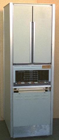
(The above photo and the front-panel photo below are from
Paul
Pierce’s PDP-8 collection.)
The Front Panel
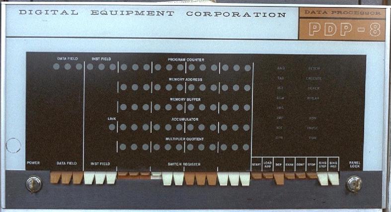
The round gray spots in the middle and the light gray lettering on the right have incandescent
light bulbs behind them. They light up to show the contents of the various hardware
registers, which is useful when single-stepping for debugging purposes. It’s
also fun to write tricky programs that make the lights light up in ways that
humans find
amusing. 8-)
In addition to twelve data switches, called the switch register, there are:
| START |
Start |
Begin program execution |
| LOAD ADD |
Load Address |
Load program counter from switch register |
| DEP |
Deposit |
Store switch register into memory addressed by program counter |
| EXAM |
Examine |
Load accumulator from memory addressed by program counter
(The contents of the accumulator would be visible on front-panel lights.)
|
| CONT |
Continue |
Resume program execution |
| STOP |
Stop |
Halts program execution at the end of the current instruction |
| SING STEP |
Single Step |
When up, causes CONT to execute just one memory cycle |
| SING INST |
Single Instruction |
When up, causes CONT to execute just one instruction |
To the left of the switch register, there are six additional switches,
three for the data field and three for the instruction field, which also
get loaded when the user hits LOAD ADD.
(A field is a 4k block of memory. The PDP-8
can have up to eight of them.)
The PDP-8 Instruction Set
PDP-8 instructions use three bits for the opcode. There are six
memory-reference instructions with opcodes 0 through 5, I/O instructions
with opcode 6, and operate microinstructions, which perform
a variety of operations on hardware registers, with opcode 7.
Given the 12-bit word length, when thinking about the PDP-8,
think octal.
| Memory-Reference Instructions |
| 0 |
1 |
2 |
3 |
4 |
5 |
6 |
7 |
8 |
9 |
10 |
11 |
| Opcode |
I |
P |
Address |
|
| Opcode |
Mnemonic |
Meaning |
| 0 |
AND |
Bitwise and |
| 1 |
TAD |
Two’s-complement add |
| 2 |
ISZ |
Increment, skip if zero |
| 3 |
DCA |
Deposit and clear the accumulator |
| 4 |
JMS |
Jump to subroutine |
| 5 |
JMP |
Jump |
|
| I |
0 |
Direct addressing |
| 1 |
Indirect addressing |
| P |
0 |
Page 0 |
| 1 |
The page from which the instruction was fetched |
|
|
|
|
|
| I/O Instructions |
| 0 |
1 |
2 |
3 |
4 |
5 |
6 |
7 |
8 |
9 |
10 |
11 |
| 6 |
Device |
Pulse |
|
| Some Canonical Device Assignments |
|---|
| Device
| Used For
|
| 00 |
Internal CPU control |
| 01 |
High-speed paper tape reader |
| 02 |
High-speed paper tape punch |
| 03 |
TTY keyboard, low-speed paper tape reader |
| 04 |
TTY printer, low-speed paper tape punch |
| 2x |
Extended memory unit |
| 60-62 |
DF32D random-access disk drive |
| 76,77 |
DECTAPE random-access tape drive |
|
| A Few Examples |
|---|
| Device |
Pulse |
Mnemonic |
Operation
|
| 00 |
1 |
ION |
Interrupts on |
| 2 |
IOF |
Interrupts off |
| 01 |
1 |
RSF |
Skip on high-speed paper tape reader flag |
| 2 |
RRB |
Bitwise-or HS reader buffer into accumulator |
| 4 |
RCF |
Clear HS reader flag, begin reading next character |
| 03 |
1 |
KSF |
Skip on TTY keyboard flag |
| 2 |
KCC |
Clear accumulator and TTY keyboard flag,
begin reading low-speed paper tape reader |
| 4 |
KRS |
Bitwise-or keyboard buffer into accumulator |
| 6 |
KRB |
Microcoded KCC KRS |
| 04 |
1 |
TSF |
Skip on TTY printer flag |
| 2 |
TCF |
Clear TTY printer flag |
| 4 |
TPC |
Write accumulator to TTY printer |
| 6 |
TLS |
Microcoded TCF TPC |
| 2x |
1 |
CDF |
Change data field to x |
| 2 |
CIF |
Change instruction field to x |
| 3 |
CDF CIF |
Change both fields to x |
| 21 |
4 |
RDF |
Read data field into accumulator bits 6–8 |
| 22 |
RIF |
Read instruction field into accumulator bits 6–8 |
|
CDF takes effect immediately. The data field is used
only for computing the effective address when doing indirect
addressing. Directly addressed operands, and indirect addresses
themselves, are accessed from the current instruction field.
|
|
CIF just saves the new field number in an internal
register. The new instruction field doesn’t actually
take effect until the next JMP or JMS
instruction.
|
|
| Operate Microinstructions |
| 0 |
1 |
2 |
3 |
4 |
5 |
6 |
7 |
8 |
9 |
10 |
11 |
| 7 |
0 |
CLA |
CLL |
CMA |
CML |
RAR |
RAL |
0 |
IAC |
| RTR |
RTL |
1 |
| 1 |
*SMA |
*SZA |
*SNL |
*0 |
OSR |
HLT |
0 |
| *SPA |
*SNA |
*SZL |
*1 |
| **MQA |
|
**MQL |
|
|
|
**1 |
|
* With bit 8 clear, SMA,
SZA and SNL are logically ored to
determine whether to skip. With bit 8 set, SPA,
SNA and SZL are logically anded;
and bits 5, 6 and 7 all clear with bit 8 set yields an
unconditional skip.
|
|
** Available only with optional multiplier/quotient
(MQ) register. The extended arithmetic element (EAE) option
expands on these instructions greatly.
|
|
| Mnemonic | Sequence | Operation |
|---|
| Group 1 (bit 3 clear) |
|---|
|
CLA
|
1 |
Clear the accumulator
|
|
CLL
|
1 |
Clear the link
|
|
CMA
|
2 |
Complement the accumulator
|
|
CML
|
2 |
Complement the link
|
|
RAR
|
4 |
Rotate accumulator and link right
|
|
RAL
|
4 |
Rotate accumulator and link left
|
|
RTR
|
4 |
Rotate twice right
|
|
RTL
|
4 |
Rotate twice left
|
|
IAC
|
3 |
Increment the accumulator
|
| Group 2 (bit 3 set, bit 11 clear) |
|---|
|
CLA
|
2 |
Clear the accumulator
|
|
SMA
|
1 |
Skip on minus accumulator
|
|
SPA
|
1 |
Skip on positive accumulator
|
|
SZA
|
1 |
Skip on zero accumulator
|
|
SNA
|
1 |
Skip on non-zero accumulator
|
|
SNL
|
1 |
Skip on non-zero link
|
|
SZL
|
1 |
Skip on zero link
|
|
OSR
|
3 |
Bitwise-or switch register into accumulator
|
|
HLT
|
3 |
Halt
|
| Group 3 (bits 3 and 11 set) |
|---|
|
CLA
|
1 |
Clear the accumulator
|
|
MQA
|
2 |
Bitwise-or MQ with accumulator
|
|
MQL
|
2 |
load MQ from accum., then clear accum.
|
| Some common combinations have mnemonics of their own |
|---|
| Mnemonic | For | Operation |
|---|
|
CIA
|
CMA IAC
|
Complement and increment accumulator
(two’s-complement negation)
|
|
LAS
|
CLA OSR
|
Load accumulator from switch register
|
|
STL
|
CLL CML
|
Set the link
|
|
GLK
|
CLA RAL
|
Get the link (into accumulator LSB)
|
|
CAM
|
CLA MQL
|
Clear accumulator and multiplier/quotient
|
|
SWP
|
MQA MQL
|
Swap accumulator and multiplier/quotient
|
|
ACL
|
CLA MQA
|
Load accumulator from multiplier/quotient
|
| Other Instructions |
|---|
| Mnemonic | Instruction | Operation |
|---|
|
NOP
|
7000 |
No operation.
|
|
BSW
|
e.g., 7002 |
(Bits 3, 8 and 9 clear; bit 10 set.)
Swap 6-bit bytes in accumulator.
|
|
SKP
|
e.g., 7410 |
(Bits 5, 6, 7 and 11 clear; bits 3 and 8 set.)
Unconditional skip.
|
|
Here’s a cute little PDP-8 program.
This program clears all memory in the current instruction field, including itself, to zero.
It’s not an algorithm because it doesn’t halt. Also, it doesn’t work
in general...at one point it tries to execute the undefined 7777 instruction, which
originally was effectively a no-op, but could hang later processors with
some EAE models.
Here’s one possible version
of “HELLO, WORLD.”
| Location |
Contents |
Instruction |
Comments |
| 0000 |
7200 |
CLA |
Get next character |
| 0001 |
1410 |
TAD I 10 |
| 0002 |
7450 |
SNA |
Null byte? |
| 0003 |
7402 |
HLT |
Yes: halt |
| 0004 |
6046 |
TLS |
No: print it |
| 0005 |
6041 |
TSF |
Wait for printing done |
| 0006 |
5005 |
JMP 5 |
| 0007 |
5000 |
JMP 0 |
Loop |
| 0010 |
0010 |
Next char addr in auto-increment location |
| 0011 |
0110 |
’H’ |
|
| 0012 |
0105 |
’E’ |
| 0013 |
0114 |
’L’ |
| 0014 |
0114 |
’L’ |
| 0015 |
0117 |
’O’ |
| 0016 |
0054 |
’,’ |
| 0017 |
0040 |
’ ’ |
| 0020 |
0127 |
’W’ |
| 0021 |
0117 |
’O’ |
| 0022 |
0122 |
’R’ |
| 0023 |
0114 |
’L’ |
| 0024 |
0104 |
’D’ |
| 0025 |
0056 |
’.’ |
| 0026 |
0015 |
(CR) |
It takes three character times
at 300 baud to physically return
the carriage on an ASR33. 8-)
|
| 0027 |
0012 |
(LF) |
| 0030 |
0377 |
(RUBOUT) |
| 0031 |
0000 |
(NUL) |
|
An important part of the PDP-8 canon is the program called the RIM loader.
This program, which would be toggled into the computer with the
front-panel switches, loads a program into memory
from a paper tape in “RIM” format
(address, data, address, data). The program most commonly loaded would be
the BIN loader, which loads yet another paper tape in the more efficient,
and more interesting, “BIN” format
described below.
Toggle in the RIM loader, load the BIN loader, load your program. Bootstrap
loaders are for sissies. 8-)
12-bit addresses and data would be represented by the 6 LSBs of pairs of
consecutive characters, with addresses identified by a 1 in the next-to-most
significant bit of the first character in the pair. Thus, addresses were pairs
of characters of the form, 01 xxx xxx/00 xxx xxx;
data were 00 xxx xxx/00 xxx xxx pairs. Any character
with a 1 in the MSB, if read when expecting the first character of a pair,
would simply be ignored. This allowed manually making corrections with RUBOUTs
(11 111 111).
Here’s what might be on a paper tape to load location
12348 with the number 55338:
| Binary |
Octal |
Notes |
| 01 001 010 |
112 |
First byte of address
has bit 1 (from left) set |
| 00 011 100 |
034 |
| 11 111 111 |
377 |
RUBOUT rubs out a mistake I made |
| 00 101 101 |
055 |
The two bytes of data |
| 00 011 011 |
033 |
Following is the version for the low-speed paper tape reader attached to the
teletype.
Like the first program above, it never halts, but just gets stuck in a tight
loop when the tape ends. You hit the front panel STOP switch when
it’s done.
| Location |
Contents |
Instruction |
Comments |
| 7756 |
6032 |
KCC |
Clear accumulator and keyboard flag;
begin reading next paper tape position |
| 7757 |
6031 |
KSF |
Wait for next character |
| 7760 |
5357 |
JMP 7757 |
| 7761 |
6036 |
KRB |
Clear accumulator and read 8 bits;
begin reading next paper tape position |
| 7762 |
7106 |
CLL RTL |
Shift left 4 bits |
| 7763 |
7006 |
RTL |
| 7764 |
7510 |
SPA |
MSB zero? |
| 7765 |
5357 |
JMP 7757 |
No, ignore (probably a RUBOUT) |
| 7766 |
7006 |
RTL |
7 LSBs now in link and upper 6 accumulator bits
(if link set, first 6-bit byte of address, else data)
|
| 7767 |
6031 |
KSF |
Wait for next byte |
| 7770 |
5367 |
JMP 7767 |
| 7771 |
6034 |
KRS |
Bitwise-or second byte into lower 6 bits |
| 7772 |
7420 |
SNL |
Address or data? |
| 7773 |
3776 |
DCA I 7776 |
Store data |
| 7774 |
3376 |
DCA 7776 |
Store address (if data, new address follows anyway) |
| 7775 |
5356 |
JMP 7756 |
|
| 7776 |
---- |
|
Temp. storage for address |
| 7777 |
(reserved for BIN loader’s starting address)
|
Here’s the high-speed reader version. Note the tricky code at
location 7765: since this modifies the saved address, sequences of
error-erasing RUBOUTs must begin with addresses.
An early version instead had a CLA in location 7755, which was
neither necessary (the front-panel START switch clears the
accumulator) nor correct (too many RCFs when looping because
of a RUBOUT); but this explains
why the BIN loader doesn’t use 7755.
| Location |
Contents |
Instruction |
Comments |
| 7756 |
6014 |
RCF |
Clear high-speed reader flag;
begin reading next paper tape position |
| 7757 |
6011 |
RSF |
Wait for next character |
| 7760 |
5357 |
JMP 7757 |
| 7761 |
6016 |
RRB RCF |
Read character; clear flag and
begin reading next paper tape position |
| 7762 |
7106 |
CLL RTL |
Shift left 4 bits |
| 7763 |
7006 |
RTL |
| 7764 |
7510 |
SPA |
MSB zero? |
| 7765 |
5374 |
JMP 7774 |
No, ignore (probably a RUBOUT)
Tricky code: since RCF doesn’t clear the AC,
we JMP to a DCA and then loop.
|
| 7766 |
7006 |
RTL |
7 LSBs now in link and upper 6 accumulator bits
(if link set, first 6-bit byte of address, else data)
|
| 7767 |
6011 |
RSF |
Wait for next byte |
| 7770 |
5367 |
JMP 7767 |
| 7771 |
6016 |
RRB RCF |
Bitwise-or second byte into lower 6 bits; clear flag
and begin reading next paper tape position |
| 7772 |
7420 |
SNL |
Address or data? |
| 7773 |
3776 |
DCA I 7776 |
Store data |
| 7774 |
3376 |
DCA 7776 |
Store address (if data, new address follows anyway) |
| 7775 |
5357 |
JMP 7757 |
|
| 7776 |
---- |
|
Temp. storage for address |
| 7777 |
(reserved for BIN loader’s starting address)
|
The BIN loader is somewhat more interesting.
- It reads from either the low-speed or high-speed paper tape reader
as selected by a front-panel switch.
- Rather than simply ignoring RUBOUTs, it ignores
anything between pairs of RUBOUTs. Thus you
can wipe out a whole section of a tape by punching RUBOUTs
over just the first and last punches of the section.
- It can load code into any memory field.
- It maintains a checksum.
- It halts after reading a final checksum,
keeping the resulting checksum in the accumulator,
which can be observed on front-panel lights.
If all goes well, no accumulator light will be lit. 8-)
The canonical starting address is 7777 which just contains
a JMP instruction to the actual initialization code.
After loading the BIN loader, you stick the paper tape for your program in the
reader, load address 7777, maybe turn off the most significant front-panel switch
if you’re using the high-speed reader, then hit the START switch.
In addition to the 1xx/0xx address characters
and 0xx/0xx data characters also recognized by
the RIM loader, the BIN loader recognizes:
- 377 exactly (RUBOUT)
- 3dx (but not 377, usually 3d0) to request data field d
- 2xx (usually 200) as a header or trailer
2xx characters are simply ignored until an address or data is encountered.
Once past the first address or data, the next 2xx will cause a branch
to the shutdown code, and the previous pair of characters
won’t be stored, but rather will be interpreted as a checksum.
Folks who like tricky, self-modifying spaghetti code will appreciate some parts of the BIN loader:
/
/ Uninitialized temp. storage:
/
7612 ----	/ RUBOUT flag (always 0 or 7777)
7613 ----	/ current CDF instruction
7614 ----	/ most recent input char
7615 ----	/ checksum
7616 ----	/ current address

/ 7617 through 7625 unused

/
/ The following subroutine reads the first character of a pair.
/ It ignores anything between pairs of RUBOUTs and handles changing the data field.
/
/ Tricky code:  if it reads a header or trailer (2xx), it just returns normally,
/ which gets to a JMP instruction that just loops right back (header) or jumps to
/ the halt code (trailer); otherwise, for an address or data byte (the usual case),
/ it ISZs its return address to get past that JMP.
/
7626 ----		/ return address

7627 3212 DCA 7612	/ AC 0 on entry...reset RUBOUT flag

7630 4260 JMS 7660	/ read a char into AC and 7614
7631 1300 TAD 7700	/ why add HLT instruction?  because it happens to be -376
7632 7750 SPA SNA CLA	/ was the char 377 (RUBOUT)?
7633 5237 JMP 7637	/ no
7634 2212 ISZ 7612	/ yes, was RUBOUT flag 7777?
7635 7040 CMA		/ no, make AC 7777 to store in RUBOUT flag
7636 5227 JMP 7627	/ else leave AC 0; and in any event, loop storing RUBOUT flag

7637 1212 TAD 7612	/ char was not RUBOUT; get RUBOUT flag
7640 7640 SZA CLA	/ even number of RUBOUTs?
7641 5230 JMP 7630	/ no, ignore until we get another

7642 1214 TAD 7614	/ get char
7643 0274 AND 7674	/ mask 0300 (two MSBs of char)
7644 1341 TAD 7741	/ why add group-2 CLA?  because it happens to be -200
7645 7510 SPA		/ at least 0200?
7646 2226 ISZ 7626	/ no, increment return address (can’t skip)
7647 7750 SPA SNA CLA	/ at least 0300?
7650 5626 JMP I 7626	/ no, return
			/ yes, data field request:
7651 1214 TAD 7614	/ get char
7652 0256 AND 7656	/ mask mem. field bits
7653 1257 TAD 7657	/ make new CDF instruction
7654 3213 DCA 7613	/ save it for later
7655 5230 JMP 7630

/
/ Static data:
/
7656 0070		/ memory field bit mask
7657 6201 CDF 0		/ archetypal CDF instruction

/
/ The following subroutine reads the next character from the paper tape
/ into the accumulator and location 7614.
/
7660 ----		/ return address

7661 ----		/ will become JMP 7662 low-speed or JMP 7670 high-speed

7662 6031 KSF
7663 5262 JMP 7662	/ wait for low-speed reader
7664 6036 KRB		/ read a byte, begin reading next

7665 3214 DCA 7614	/ save byte
7666 1214 TAD 7614	/ get it back in AC
7667 5660 JMP I 7660	/ return

7670 6011 RSF
7671 5270 JMP 7670	/ wait for high-speed reader
7672 6016 RRB RCF	/ read a byte, begin reading next
7673 5265 JMP 7665

/
/ More data:
/
7674 0300		/ mask for two MSBs of char

/
/ The end game:
/
7675 4343 JMS 7743	/ assemble two 6-bit chars
7676 7041 CIA		/ negate
7677 1215 TAD 7615	/ add checksum
7700 7402 HLT		/ checksum (presumably zero) visible
			/ in front-panel accumulator lights

/
/ Initialization:
/
7701 6032 KCC		/ clear AC, reset LS and HS reader flags,
7702 6014 RCF		/ and begin reading (don’t know from which yet)

7703 6214 RDF		/ current data field into AC(6-8)
7704 1257 TAD 7657	/ make CDF instruction
7705 3213 DCA 7613	/ save it for later

7706 7604 LAS		/ read front-panel switches into AC
7707 7700 SMA CLA	/ high-speed reader?
7710 1353 TAD 7753	/ yes, add 6
7711 1352 TAD 7752	/ add JMP 7662
7712 3261 DCA 7661	/ save either JMP 7662 or JMP 7670

7713 4226 JMS 7626	/ read 1st char
7714 5313 JMP 7713	/ loop until subr. ISZs its return addr.

/
/ Here begins the main loop.  The accumulator will be 0, thus initializing
/ the checksum, when we fall through from the startup code immediately above.
/
7715 3215 DCA 7615	/ store checksum

7716 1213 TAD 7613	/ get CDF instruction
7717 3336 DCA 7736	/ save it

7720 1214 TAD 7614	/ get input char
7721 3354 DCA 7754	/ save it
7722 4260 JMS 7660	/ read 2nd char into AC and 7614
7723 3376 DCA 7776	/ save it

7724 4226 JMS 7626	/ read another 1st char
7725 5275 JMP 7675	/ if subr. didn’t ISZ its return addr., goto halt code

7726 4343 JMS 7743	/ assemble two 6-bit chars.
7727 7420 SNL		/ address?
7730 5336 JMP 7736	/ no
7731 3216 DCA 7616	/ yes, save addr.

7732 1354 TAD 7754	/ add 1st char
7733 1376 TAD 7776	/ add 2nd char
7734 1215 TAD 7615	/ add previous checksum
7735 5315 JMP 7715	/ loop

7736 ----		/ becomes CDF whatever
7737 3616 DCA I 7616	/ store data
7740 2216 ISZ 7616	/ next address
7741 7600 CLA		/ Tricky code:  we need a no-op here that the ISZ can skip
			/ if the address we just loaded happens to be 7777.  A CLA
			/ will do because it doesn’t do anything that the DCA hasn’t
			/ already done; and a group-2 CLA happens to have the value,
			/ -200, which is used above.
7742 5332 JMP 7732	/ go figure new checksum

/
/ The following subroutine assembles two characters into a 12-bit word
/ with the address indicator bit in the link.
/
7743 ----
7744 1354 TAD 7754
7745 7106 CLL RTL
7746 7006 RTL
7747 7006 RTL
7750 1376 TAD 7776
7751 5743 JMP I 7743

/
/ More data:
/
7752 5262 JMP 7662	/ JMP instruction for selecting low-speed reader
7753 0006		/ augend for above JMP’s address for high-speed reader
7754 ----		/ temp. storage for 1st char

/
/ 7755 through 7775 reserved for RIM loader
/

7776 ----		/ temp. storage for 2nd char (shared by RIM loader)
7777 5301 JMP 7701
PDP-8 Internals
This author was a wires-and-pliers guy when he first encountered the PDP-8.
He’s a programmer now, in no small part because of the fun
he had with the PDP-8 8-);
but he retains an interest in how things really work.
(OK, not “really” down to the quantum level;
but you know what’s meant.)
The Hardware Registers
| Name |
Size
(bits) |
Description |
Use |
| PC |
12 |
Program Counter |
Holds address of next instruction |
| MA |
12 |
Memory Address Register |
Holds address of memory location currently being accessed |
| MB |
12 |
Memory Buffer |
All data in and out of memory go through this register |
| IR |
3 |
Instruction Register |
Saves instruction opcodes across major states |
| DF |
3 |
Data Field |
Upper three bits of 15-bit address when indirectly accessing data |
| IF |
3 |
Instruction Field |
Upper three bits of 15-bit address when fetching instructions
or directly accessing data |
| IB |
3 |
Instruction Buffer |
Holds new IF until next JMP or JMS |
| AC |
12 |
Accumulator |
Where arithmetic happens |
| L |
1 |
Link |
Overflow bit for accumulator |
| MQ |
12 |
Multiplier/Quotient Register |
Optional fast storage for partial products, etc. |
The Six Major States
(Each corresponds to a magnetic core memory
read-write
cycle.)
Program
Execution |
FETCH |
Fetch instruction; execute I/O instructions, microinstructions
and JMP direct.
|
| DEFER |
Get indirect addresses; execute JMP indirect.
|
| EXECUTE |
Execute memory-reference instructions other than JMP.
|
“Data
Break”
(DMA) |
WC |
Word count
|
| CA |
Current address
|
| B |
Break (data transfer)
|
Operation
Flow diagrams for:
The flow diagrams show basically what happens when one of the START,
LOAD ADD, DEP, EXAM or CONT
switches is pressed, when an instruction is executed, or when a peripheral does
a “data break” (like DMA,
but under control of the processor, not the peripheral).
| The Arrow Symbols on the Diagrams |
1 —> flip-flop
0 —> flip-flop |
Set or clear the flip-flop |
| 0 —> register |
Clear the register |
| +1 —> register |
Increment the contents of the register |
| regx —> regy |
Bitwise-or regx into regy |
| regx -j-> regy |
(Actually a solid arrow with an overstruck ‘j’)
“Jam transfer” (transfer both 1s and 0s) |
When
one of the switches is pressed, things happen at one of four times,
SP0 through SP3. Everything shown at
a particular time basically begins at the same time and takes
a non-zero amount of time to complete; so,
for example, when we see PC-j->MA and
+1—>PC both at SP1,
MA gets the value that was in PC before the
incrementing.
Note that most register-to-register transfers are bitwise-ors,
which made the hardware cheaper to build; so, for example, when we load the program counter
from the switch register, we first clear PC at SP1,
then or-transfer SR into PC at SP2.
Note also that the DEP and EXAM switches, after initializing
some registers, run the EXECUTE major state of a
DCA or a TAD, respectively.
When
a program is running, things happen on each edge of a
two-phase clock. The four times, called T1A, T1B,
T2A and T2B, correspond to the horizontal dotted lines
(or the bottom of the page in the case of T2B) on the flow diagram.
The basic idea for a core memory read-restore cycle (i.e., “major state”):
In more detail:
- At T1A, the memory addressed by MA is
destructively
read into MB.
- In the FETCH major state, the instruction’s
opcode is also loaded into IR.
- In the EXECUTE major state, the DCA and JMS
instructions refrain from modifying MB.
- At T1B, any necessary changes to the memory location are
put in MB.
- At T2A, the location addressed by MA is
restored from MB, and a new MA value might be
computed.
- At T2B, we mostly just get ready for the next major state
(clear MB and IR, for example),
except
that some operations that don’t alter memory might complete:
- In the FETCH major state, some operate microinstructions
and JMP direct actually finish their work.
- In the DEFER major state, JMP indirect
actually finishes its work.
- In the EXECUTE major state:
- The AND instruction finally does the deed.
- The TAD instruction propagates the carries
generated by the half add at T1B.
Some I/O instructions would set a “pause” flip-flop
that would temporarily halt the clock, and thus memory cycles,
to allow time for signals to propagate between the CPU and its
peripherals, or for the peripherals to do some task that took
more than one memory cycle to complete.
A Simple Example:
Let’s say we’ve loaded the program:
	0200	7001	IAC
	0201	1250	TAD 250
	0202	7402	HLT
	...
	0250	0005
Here’s some of what happens when we set the switch register to 0200
then hit LOAD ADD and START.
(Changes are shown with a gray background. Core memory
destructive read/restore not shown.)
| Operation |
Time |
RUN |
Major
State |
PC |
MA |
(MA) |
MB |
IR |
AC |
Comments |
| LOAD ADD |
SP0 |
0 |
- |
---- |
---- |
|
---- |
- |
---- |
0—>RUN |
| SP1 |
0 |
- |
0000 |
---- |
|
---- |
- |
---- |
0—>PC |
| SP2 |
0 |
- |
0200 |
---- |
|
---- |
- |
---- |
SR—>PC |
| SP3 |
0 |
- |
0200 |
---- |
|
---- |
- |
---- |
|
| START |
SP0 |
0 |
- |
0200 |
---- |
|
---- |
- |
---- |
0—>RUN |
| SP1 |
0 |
FETCH |
0200 |
0200 |
7001 |
0000 |
0 |
0000 |
0—>AC; 0—>MB; 0—>IR; 1—>F; PC-j->MA |
| SP2 |
0 |
FETCH |
0200 |
0200 |
7001 |
0000 |
0 |
0000 |
Get ready for memory cycles |
| SP3 |
1 |
FETCH |
0200 |
0200 |
7001 |
0000 |
0 |
0000 |
1—>RUN |
| IAC |
T1A |
1 |
FETCH |
0200 |
0200 |
7001 |
7001 |
7 |
0000 |
(MA)—>MB; MB(0—2)transitions—>IR |
| T1B |
1 |
FETCH |
0201 |
0200 |
7001 |
7001 |
7 |
0000 |
+1—>PC |
| T2A |
1 |
FETCH |
0201 |
0201 |
1250 |
7001 |
7 |
0000 |
PC-j->MA |
| T2B |
1 |
FETCH |
0201 |
0201 |
1250 |
0000 |
0 |
0001 |
+1—>AC; 0—>MB; 0—>IR; 1—>F |
| TAD 250 |
T1A |
1 |
FETCH |
0201 |
0201 |
1250 |
1250 |
1 |
0001 |
(MA)—>MB; MB(0—2)transitions—>IR |
| T1B |
1 |
FETCH |
0202 |
0201 |
1250 |
1250 |
1 |
0001 |
+1—>PC |
| T2A |
1 |
FETCH |
0202 |
0250 |
0005 |
1250 |
1 |
0001 |
MB(5—11)-j->MA |
| T2B |
1 |
EXECUTE |
0202 |
0250 |
0005 |
0000 |
1 |
0001 |
0—>MB; 1—>E |
| T1A |
1 |
EXECUTE |
0202 |
0250 |
0005 |
0005 |
1 |
0001 |
(MA)—>MB; |
| T1B |
1 |
EXECUTE |
0202 |
0250 |
0005 |
0005 |
1 |
0004 |
MB half add to AC |
| T2A |
1 |
EXECUTE |
0202 |
0202 |
7402 |
0005 |
1 |
0004 |
PC-j->MA |
| T2B |
1 |
FETCH |
0202 |
0202 |
7402 |
0000 |
0 |
0006 |
AC carry; 0—>MB; 0—>IR; 1—>F |
| HLT |
T1A |
1 |
FETCH |
0202 |
0202 |
7402 |
7402 |
7 |
0006 |
(MA)—>MB; MB(0—2)transitions—>IR |
| T1B |
0 |
FETCH |
0203 |
0202 |
7402 |
7402 |
7 |
0006 |
+1—>PC; 0—>RUN |
| T2A |
0 |
FETCH |
0203 |
0203 |
|
7402 |
7 |
0006 |
PC-j->MA |
| T2B |
0 |
FETCH |
0203 |
0203 |
|
0000 |
0 |
0006 |
0—>MB; 0—>IR; 1—>F |
For more information, seeChapter 2 of the
PDP-8
Maintenance Manual.
All suggestions and corrections will be welcome; all flames will be amusing.
Mail to was at pobox dot com.